Q. Explain the advantages of building an intergrated circuit with a small line width
1.1 Moor's Law

According a Moor's law, the number of transistor on a microchip doubles every two year
what are the benefits of this chip getting smaller?
1.2 Size of Wafer and Critical Dimension(CD)
- What is the CD ?
Minimum length between Source and Drian( = Gate Length )
if this distance is short, Switching is possible even with Low ennergy and Low Voltage
-> Improved switching performance

1.3 Why make it small ?
First, if you make it smaller, you can make more chip in the same area
More chip can be made in the same size wafer for the same time

Second, if you make it smaller, circuit resistance is changed
you can make a chip with excellent performance(Velocity, Power consumption, Fever ... ) from s
44ame die
-> The Resistance is inversely proprotional to the line width of the circuit so Response speed get faster

Third, Edge effect, Chip is getting smaller, the smaller the edge area
As the percentage of surviving chips, so does the yield

Making it small is not just about trying be cool or showing off, but
about practical performance and price competition
1.4 What is the Step of Semiconductor chip fabrication
Step.1 Wafer Preparation
Includes crystal growing, Rounding, Slicing and polishing

Step.2 Wafer Fabrication
includes cleaning, latering, patterning, etching and doping

Step.3 Test/Sort includes
probing, testing and sorting of each die on the wafer

Step.4 Assembly and Packaging
The wafer is cut along scribe lines to separate each die
Metal connections are made and the chip in encapsulated

Step.5 Final Test ensures IC
Passes electrical and environment testing

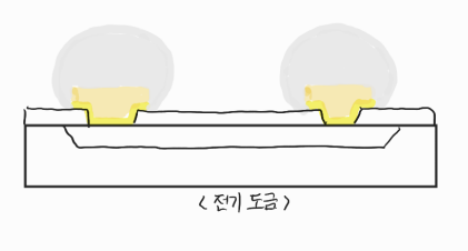
Q. Explain the Bumping process,
Bumping process
It is a process of forming and connecting protrusion-shaped metals(Bump)
rather than the existing wire bonding.채너
Step.1 UBM sputtering

Depostion UBM(Under Bump Metallugy) through a sputtering of wafer
- UBM : It is a Multi-Layer Metal formed between the electrode the bump the prevent channel diffusion
Step.2 PR patterning

A pattern is formed by excluding areas in which bumps are to be formed by the Photoresist
Step.3

Depostion a Bump used a plating solution
Step.4

Etch the Photo resist and BUM
Step.5 Final
make a Ball bump by reflow
Compared to the exsiting wrie bonding method, the Flip chip bonding method
electrical performance is excellent as the length of the connection between the chip and
it is possible to increase the degree of integration of input/output terminals
by dissipating heat, the heat inside is quickly released to the outside